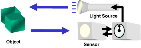
TOF range imaging is one of 3-D image capture methods and the range L is determined by sensing the roundtrip time of flight for the light.
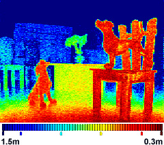
A pixel structure of the sensor employs single layer polysilicon gates on thick field oxide. Using these single layer polysilicon gates, the sensor achieves high-speed charge transfer essential for TOF range imaging like CCD and can divide signal charge depending on delay time into two floating diffusion (FD) in each pixel (x-x direction). small duty cycle for the transfer gates and light source control pulse and the charge draining structure (y-y direction) drastically reduce the effect of background illumination. Using this sensor, we can get a video rate (30fps) gray scale image and range image, simultaneous. The minimum range resolution at 30frames/s and the light pulse width of 25ns is 5.0mm. The resolution at 3frames/s, which corresponds to the averaging with 10 samples, is 1.7mm.
|
|
| |
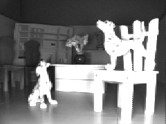
| Pixel Circuit for TOF Range Image Sensor | Gray Scale Image | Range Image |
Automobile, Robot vision systems, Security, Medical and so on.